
The supported features are:
- Sector read in all formats
- Audio track playback including subchannel Q emulation
- Multiple disc images on the same SD card (switched by removing and reinserting the card)
The design files for the hardware, and the source code for the FPGA bitstream and software, can be found on GitHub.
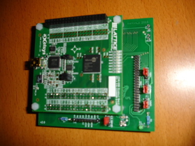
The basis for the hardware is the Lattice iCE40HX-8K FPGA, which is a simple FPGA for which a completely open-source toolchain is available. I'm using the official breakout board, but due to the SMT connector needed interface with the motherboard, there is also a custom PCB that acts as a riser. The design files and Gerbers are available on GitHub, see above.
The complete bill of materials is as follows:
|
Most of these components are generic and there is no need to pick exactly the same manufacturer or model. Be careful about the dimensions of the pin headers and sockets though, as they are matched to the spacers.
The 20x2 pin headers are for populating J3 and J4 on the breakout board. Please note that the pins should be facing downwards. The last three components are not needed for the main functionality, they implement a passthrough for connecting a slave hard drive.
In addition to these components, you will need:
- A short USB-mini cable to power the breakout board (fits into the USB-A connector on the riser board). A cable with the connectors at a right angle, such as this one is recommended due to the limited space inside the Dreamcast.
- An SD-card module, and wiring to connect it to the 9-pin header. I used this module.
- Some rubber feet to support the board inside the Dreamcast. Since the distance to the plate below differs between the corners, using stackable feet is a good idea.
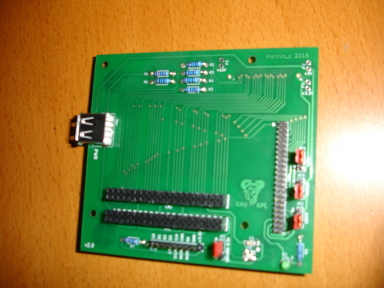
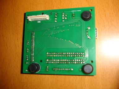
This is what the populated board will look like:
The FPGA configuration consists of several blocks, as illustrated by the following schematic:
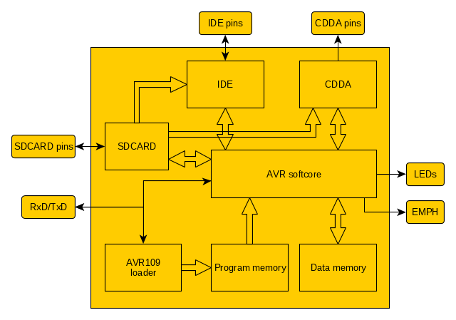 |
The AVR softcore implements the instruction set of an ATmega AVR CPU, and provides somewhere for the control logic software to run. It was developed by Ruslan Lepetenok and published on OpenCores. The Data and Program Memories are implemented using Block RAM. The Program Memory is preloaded by the bitstream, but can also be updated from the serial port using the on-board AVR109 compatible loader (which is implemented in logic, and does not run on the AVR softcore; the SPM instruction is not implemented).
The IDE block implements the standard IDE register file which is shared between the Dreamcast and the AVR softcore. It will interrupt the AVR when the Dreamcast writes to the command register, or when a transfer has completed. There is a 512 byte data buffer for PIO and DMA, which can be accessed by the AVR but also filled directly by the SDCARD block.
The CDDA block generates the digital audio signals going to the AICA system, and is used when playing audio tracks. There are two 512 byte sample buffers which are used in a ping-pong fashion to provided uninterrupted playback, and these can be accessed by the AVR as well as filled directly by the SDCARD block.
The SDCARD module currently implements SPI mode only. It has a built-in CRC16 calculator which can be used to check the CRC of a data block after a transfer.
The software runs on the AVR softcore, and processes IDE commands from the Dreamcast as well as keeping the CDDA buffers filled during audio playback. Disc sector contents, for both data reads and audio playback, are read from an image file in a FAT filesystem on the micro SD card. The image file also contains canned replies for the GET_TOC and REQ_SES commands, as well as the disc type (GD-ROM, CD-ROM XA, CD-ROM, CD-DA) to report to the Dreamcast. When no micro SD card is inserted, the software will report that there is no disc in the drive.
The current image state can be observed on the LEDs of the breakout board. If they are scanning, it means that no micro SD card is inserted. If they are all lit, it means that no disc image could be mounted from the micro SD card. Otherwise, LED0-6 will indicate the disc image number (0-127), and LED7 will show when the image is being accessed.
Image files should be named DISC0000.GI0, DISC0001.GI0 etc on the micro SD card. On power-up DISC0000.GI0 will be mounted, to switch image eject and reinsert the micro SD card. The image files are created by the tool makegdimg which is built in the tools directory. It accepts .gdi files (for GD-ROMs) and .nrg files (for MIL-CD and audio CDs) as input.
There are a few strap jumpers on the board. JP1 controls the source of the 3.3V for the micro SD card. Normally this should be set to "DC" to use the 3.3V directly from the Dreamcast's power supply. However, during development it can be useful to set it to "FPGA" instead, using USB power converted to 3.3V on the breakout board, so that the micro SD card can be used even when the Dreamcast is powered off.
JP2 and JP3 controls the voltage on the VLOGIC and VMOTOR pins of the 44-pin IDE passthrough connector. Do not set them to different voltages unless you are absolutely sure what you are doing, as the pins may be connected to each other inside the drive. JP4 controls the CSEL pin of the 44-pin IDE passthrough connection. In the "M" position it is grounded, in the "S" position it is floating.
Last modified: Wed Apr 29 08:15:19 CEST 2020